
Researchers have developed a 2D sensor chip that processes visual data more efficiently by eliminating energy-intensive steps in traditional image sensing.
Key facts
- •The LightTok chip was detailed in a study published in the journal Nature Sensors on Aug. 19.
- •The device uses a single-layer molybdenum disulfide floating-gate phototransistor to process visual data.
- •LightTok demonstrated 87.3% accuracy in image recognition tests.
- •The chip is reported to be 10 times more energy-efficient at converting light into tokens than conventional systems.
- •The current prototype is limited to a resolution of 32 by 32 pixels.
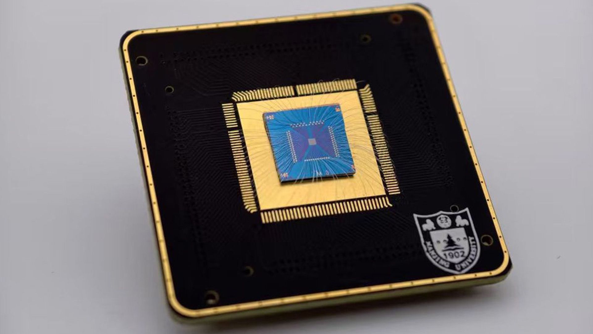
Researchers in China have developed a new 2D sensor chip called "LightTok" that converts raw light directly into tokens for artificial intelligence models. Published in the journal Nature Sensors on Aug. 19, the study details how the chip integrates sensing, memory, and computation into a single pixel. By skipping multiple energy-intensive stages required by conventional systems, the technology aims to reduce power consumption in autonomous hardware like drones.
By the numbers
How LightTok Works
Conventional visual perception systems rely on multiple stages, including analog-to-digital conversion and moving data to separate chips for processing. According to the researchers, analog-to-digital converters account for an average of 66% of an image sensor's energy consumption. LightTok addresses this by using a single-layer molybdenum disulfide floating-gate phototransistor. This material reacts to light and can trap electrical charges, allowing the chip to sense, remember, and compute data simultaneously within the same pixel. Liang Shi-Jun, a physics professor at Nanjing University, noted that the design physically eliminates data movement, which is a primary source of energy waste. The chip is named "LightTok" because it effectively allows light to enter and tokens to emerge directly.
Performance and Future Scalability
In testing, the LightTok chip achieved 87.3% accuracy in image recognition while proving to be 10 times more energy-efficient than conventional multi-step processes. However, the current prototype has a maximum resolution of only 32 by 32 pixels, which is significantly lower than the capabilities of standard smartphone cameras or sensors currently used in autonomous hardware. Miao Feng, director of Nanjing University's Institute of Brain-Inspired Intelligence, stated that the technology could potentially be scaled using the complementary metal-oxide-semiconductor (CMOS) manufacturing process. If successful, this could allow drones to operate for longer periods by reducing the energy required for visual processing.
Advertisement
This article was independently rewritten by ManyPress editorial AI from reporting originally published by Live Science.